If you are a designer or engineer working in the electronics field, you know how essential it is to ensure the signal and power integrity and management of electromagnetic interference (EMI) in your PCB and IC package designs. The good news is that HIGH TECHNOLOGY SYSTEMS now has a state-of-the-art solution to meet these needs: Ansys SIwave.
Ansys SIwave is specialised simulation software designed to offer engineers and designers a complete suite of tools for analysing and optimising their designs. The analysis in question covers several key areas such as:
- Impedance/Crosstalk/EMI Scanner
- DC Analysis
- Power Integrity
- Signal Integrity
- Electormagnetic Compatibility/Interference
- DDR4 Channel Compliance
- Chip-Package-System Analysis (CPS)
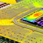
By simply importing the PCB layout (created on an ECAD), it will be possible to model, simulate and validate what has been created, both for the high-speed and power supply parts of the circuit. Post-layout analysis satisfies the designer’s need to know and improve his work prior to PCB production, through post-simulation optimisation of all layout aspects that are critical (and not) for the functioning of the entire product.
Why did we choose Ansys SIwave for our future designs? Ansys SIwave simulation software creates a wide range of benefits for us and our customers, as its correct use allows us to:
- Reduce prototyping times: as it makes it possible to analyse and optimise the layout before it is made, without having to wait for the prototypes to evaluate the changes that need to be implemented and then
start a second production of the prototypes themselves. - Reduce the time required to create a measurement system for prototypes: all measurements of interest can be made directly with the design file of your ECAD, without the use of special measurement tools.
- Reduce development costs: with the possibility of simulating prototype layouts, without the need to make them, you reduce product development costs, as you do not need to make and assemble several prototype versions of PCBs.
- Increasing the quality of the final product: with the simple testing of prototypes, the designer can never be sure that the solution he is testing is the best possible for the circuit in question; with the use of SIwave simulators, on the other hand, it is possible to achieve the highest quality of the product being manufactured, through the analysis and evaluation of all possible solutions.
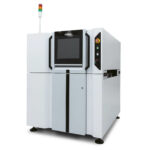
The Benefits of the AOI 3D OMRON VT-S1080:
- Unrivalled Accuracy: Thanks to its ability to work in 3D, the VT-S1080 identifies even the finest imperfections, helping to ensure the highest quality products while minimising errors.
- Faster Production: This machine is incredibly fast, allowing us to increase production without compromising quality. This allows us to meet growing market demand more efficiently and effectively.
- Reducing Production Errors: AOI 3D detects potential defects before products leave the production line, minimising waste and associated costs.
- Environmental Commitment: By reducing waste, we actively contribute to more sustainable and environmentally friendly production.
- Staff Development: This innovation has also given us the opportunity to train and further develop the skills of our team, our most valuable asset.
In a world where efficiency and quality are crucial, HTS relied on Ansys SIwave to improve its design process and achieve outstanding results. Don’t miss the opportunity to optimise your project right from the start. If you are interested in finding out more about Ansys SIwave and how it can improve your designs, contact us now at info@htsitaly.it and visit our website.